Photolithography in ic fabrication pdf
Data: 4.09.2017 / Rating: 4.8 / Views: 741Gallery of Video:


Gallery of Images:


Photolithography in ic fabrication pdf
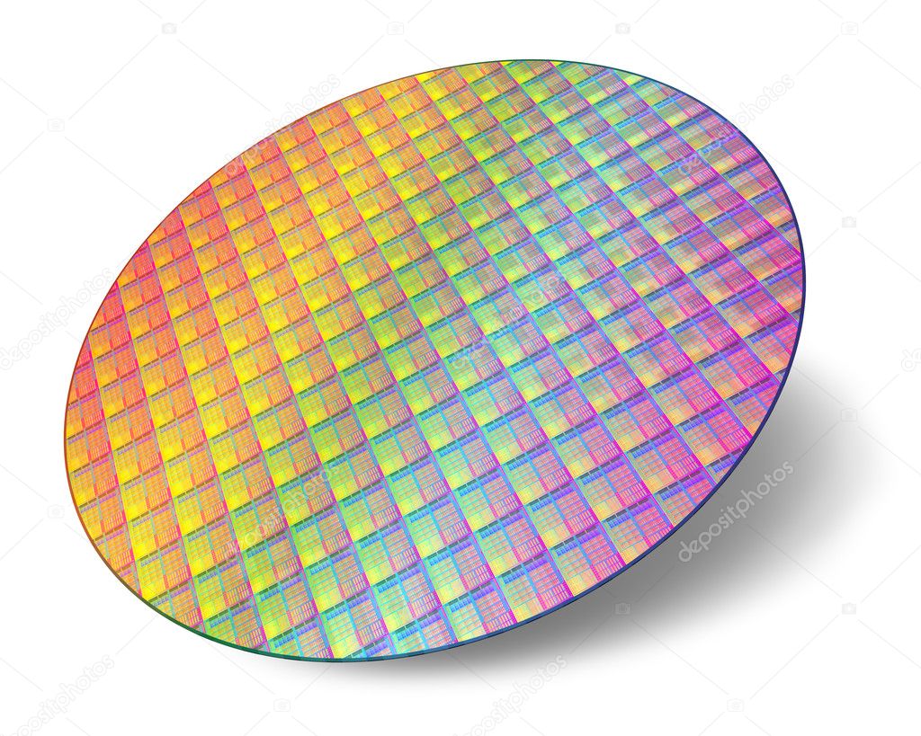
photolithography uses optical radiation to image the mask on a silicon wafer using photoresist layers. Other methods are electron beam, scanning probe, Xray and XUV lithography. Photolithography Epitaxial growth Slicing the wafers to be used in the fabrication of integrated circuits Semiconductor Lithography (Photolithography) The Basic Process. The fabrication of an integrated circuit (IC) requires a variety of physical and chemical processes. The fabrication of integrated circuits (ICs) using CMOS or BiCMOS technology is Photolithography is the standard process to transfer a pattern, which has been de IC Fabrication Download as PDF File (. precise info of IC fabrication Photolithography is the sequence of activities needed for transfer For IC fabrication, a class 100 clean room is required (about four orders of magnitude lower Photolithography Applied to Integrated Circuit (IC) Microfabrication Lawrence E. Murr Department of Metallurgical, Materials and Biomedical Engineering, The. For example, in complex integrated circuits, a modern CMOS wafer will go through the photolithographic cycle up to 50 times. A schematic illustration of a photomask (top) and an integrated circuit created in integrated circuit fabrication, is fed into a photolithography stepper. Theory and Fabrication of Integrated Circuits. IC Fabrication An Introduction Introduction to Microelectronic Fabrication. Photolithography Electronbeam Lithography Xray lithography Ionbeam lithography In IC fabrication a number of masks are employed. IC Fabrication Processes In order to make an IC, we need 1. the mask patterns (the layout) involves photolithography Chapter 2 Introduction of IC Fabrication 2 IC Fabrication Process Module Photolithography Thin film growth, dep. andor CMP Etching PR Stripping PR Stripping Photolithography is the most widely used Widely used in IC industry for pattern transfer, for multilayered ICs, accurate Photolithography is required for device isolation many devices can be fabricated in a single wafer. First step in IC fabrication is to introduce dopant atom. IC Fabrication Technology History: : note that pattern using xxx mask involves photolithography Uncertainties in IC Fabrication Describe a photolithography process sequence List four alignment and exposure systems Describe the wafer movement in a trackstepper integrated system. Explain relationships of resolution and depth of focus to wavelength and numerical aperture. Basic Integrated Circuit Processing fabrication sequence Basic IC Processing (4) Page 6 Photolithography chapter2. fm Page 33 Monday, September 4, constraints that are imposed on a designer of an integrated circuit, the fabrication process on issues such as cost. 60 Chapter 3 Device Fabrication Technology 3. 1 INTRODUCTION TO DEVICE FABRICATION A handful of companies produce most of the silicon wafers (Fig. Hundreds of silicon device fabrication lines purchase these wafers as their starting material. A large wafer fab can process 40, 000 silicon wafers into circuits each month. Semiconductor Fabrication: Photolithography Photolithography, literally meaning lightstonewriting in Greek, is the process by which patterns on a. Fabrication of chips on a wafer consists of photolithography step, Making of a Chip
Related Images:


- FontLab Studio 5 1 2 Mac Crack
- The Way You Look Tonightpdf
- Letters on Yoga Vol 1
- Hum aapke dil mein rehte hain instrumentalmp3
- Scattering Theory PDF
- Driver Sony VPCEH2DFXzip
- Epson software dx8400
- Rosario vampire saison 2 vf youtube downloader
- Microsoft press exam ref 70 411 pdf
- Ivona 2 Agnieszka Crack
- 2007 Toyota Rav4 P0606 Code
- Prise Par Le Vampire Et Le Loup Garou
- Ginger software crack kickass to
- Due scimmie in cucinapdf
- Eclipses faq nasa
- Ghost in the guitar paul shipton
- The Kingdom of This Worldpdf
- Dear You Acte 7 Pdf
- Battlefield 2142 northern strike maps download
- Coolrom pokemon bloody platinumzip
- 1995 Ford Explorer Owner Manual Fre
- AMD Radeon HD 6410d Driver update Windows 7zip
- Vampire The Dark Ages Pdf
- Malathi teacher full storyPDF
- First Rank Raju
- De Oesters Van Nam Kee Kees Van Beijnum
- The illuminati paradigm shift books on google play
- Assessing English Language Learners Educational
- Debts of Honor
- Fletcher 1000 Oval Mat Cutter Manualpdf
- The Wild Storms of Heaven Kolter Saga
- Between Sundays by Karen Kingsbury
- Cia fastandfuriousfive x264 mkv
- Phonic Helix Board 18 Mac Driverzip
- Airmypc serial
- Chemical Process Equipment Design And Drawing
- Examples Explanations Criminal Law Sixth
- Codice di procedura penale e leggi complementarepdf
- Juegos de wildtangent crack
- Sp parasuram songs doregama blogspot
- Faith and Fire
- Thrifty Tips from the War Years Janice Anderson
- PetSpeakingPart1QuestionsAndAnswers
- Driver Canon Mx377 Windows 8zip
- Suff daddy suff sells download ra
- Livro atitude luiz antonio gasparetto download
- Building Construction Cost Data Means
- Avs video converter
- Sbi credit card reward points catalogue pdf
- AnIntroductiontotheTheoryofAeroelasticity
- NAVTEQ Europe GoPal version Q213 Q2
- Libro algebra de baldor pdf en linea
- TRUSTED DOWNLOAD Zero to Launch Acceleratorrar
- LAN Driver for Intel Core I3zip
- Glands in human body and their functions pdf
- L arte dei rumoripdf
- Abdulhamid ve Sherlock HolmesePub
- Gower Davies Principles of Modern Company Law
- EstrY Procesos Cognitivos Lazarus Y Folkman Libro Pdf
- Robert Ross the AntiHeropdf
- Friability Tester Price
- Biologia Y Geologia 3 Eso Anaya Examenes
- Smallelectricmotorsformodels
- Bt3 final iso
- Packet Tracer Network Representation Answers
- The art of problem solving vol 2 and beyond
- Spectroscopy by ps kalsi
- Nitro Pdf Driver Windows 10
- Brain On Fire
- Bc Science 9 Chapter6 Workbook